 Image Credit: Justin Sullivan / Staff / Getty
 On Thursday President Donald Trump announced progress on bringing leading-edge node manufacturing to the United States. With process nodes of sub-2 nanometers in size, these are the most advanced computer chips in the world today.
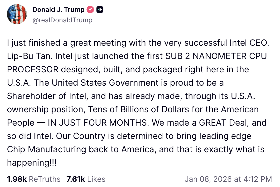
I just finished a great meeting with the very successful Intel CEO, Lip-Bu Tan. Intel just launched the first SUB 2 NANOMETER CPU PROCESSOR designed, built, and packaged right here in the U.S.A. The United States Government is proud to be a Shareholder of Intel, and has already made, through its U.S.A. ownership position, Tens of Billions of Dollars for the American People — IN JUST FOUR MONTHS. We made a GREAT Deal, and so did Intel. Our Country is determined to bring leading edge Chip Manufacturing back to America, and that is exactly what is happening!!!
While the factory Trump is speaking of is an Intel chip foundry, it is likely that other companies could contract with them to manufacture their chip architectures, such as TSMC who manufactures Apple’s chips. Ctech states:
Intel is in talks to sell its chip manufacturing operations to Taiwan’s TSMC, according to reports from Bloomberg and The New York Times. The move, which currently has the backing of the Trump administration, may involve only Intel’s U.S. manufacturing plants, but it could also extend to its facilities in Israel.
An Intel press release from August regarding the deal Trump is discussing states:
Intel Corporation today announced an agreement with the Trump Administration to support the continued expansion of American technology and manufacturing leadership. Under terms of the agreement, the United States government will make an $8.9 billion investment in Intel common stock, reflecting the confidence the Administration has in Intel to advance key national priorities and the critically important role the company plays in expanding the domestic semiconductor industry.
The government’s equity stake will be funded by the remaining $5.7 billion in grants previously awarded, but not yet paid, to Intel under the U.S. CHIPS and Science Act and $3.2 billion awarded to the company as part of the Secure Enclave program. Intel will continue to deliver on its Secure Enclave obligations and reaffirmed its commitment to delivering trusted and secure semiconductors to the U.S. Department of Defense. The $8.9 billion investment is in addition to the $2.2 billion in CHIPS grants Intel has received to date, making for a total investment of $11.1 billion.
The Semiconductor Industry Association stated in their “State of the U.S. Semiconductor Industry 2025” report:
American engineers invented semiconductors 65 years ago, and the U.S. semiconductor industry remains the global leader, commanding just over 50% of global chip revenues. But as competitors from around the world have sought to challenge U.S. leadership, America’s share of global chip manufacturing capacity was declining sharply – from 37% in 1990 to just 10% by 2022. If this trend were to continue, the U.S. semiconductor industry would risk falling back from the forefront of further advances in manufacturing processing technology, designs and architectures, and materials critical for developing the next generation of chips that will underpin the technologies of tomorrow.
Computer chips are comprised of transistors. Advancements are made by shrinking the transistor process nodes to allow more compute for a given energy input. The latest (and smallest) process node technology is known as the leading-edge node.
“In semiconductor terminology, the word ‘node’ refers to the size of the smallest feature of a transistor. In other words, the semiconductor devices used within every computer chip. Each transistor comprises of three key components; a source, a gate and a drain, which is used to amplify or switch electrical signals and power. The number of nodes that make up that transistor determines the power and capability of the device it is used in,” an article by Jordan Lorence on MRL states.
Development is currently underway for sub-2nm nodes:
As of January 6, 2026, the semiconductor industry has officially crossed the threshold into the “Angstrom Era,” a pivotal transition where transistor dimensions are now measured in units smaller than a single nanometer. This milestone is marked by a high-stakes showdown between Intel (NASDAQ: INTC) and Taiwan Semiconductor Manufacturing Company (NYSE: TSM), as both giants race to provide the foundational silicon for the next generation of artificial intelligence. While Intel has aggressively pushed its 18A (1.8nm-class) process into high-volume manufacturing to reclaim its “process leadership” crown, TSMC is readying its A16 (1.6nm) node, promising a more refined, albeit slightly later, alternative for the world’s most demanding AI workloads.
The immediate significance of this race cannot be overstated. For the first time in over a decade, Intel appears to have a credible chance of matching or exceeding TSMC’s transistor density and power efficiency. With the global demand for AI compute continuing to skyrocket, the winner of this technical duel will not only secure billions in foundry revenue but will also dictate the performance ceiling for the large language models and autonomous systems of the late 2020s.
Legacy (mature) nodes are larger transistor processes which have been perfected in years past, meaning they are easier and cheaper to manufacture with a lower rejection rate during quality control, but are generations behind the latest cutting edge node. Due to the various technology needed to manufacture each process node size, computer chip factories are built from the ground up for their specific process node.
“The ongoing trend of miniaturizing transistors, also known as reducing the process node size, is one of the defining characteristics of the semiconductor industry. As transistors continue to shrink, they enable the integration of exponentially more transistors into a single chip. This advancement brings about numerous benefits, including improved performance, reduced power consumption, and the ability to build more sophisticated on-chip architectures. These improvements are essential for the ever-expanding requirements of modern technology, ranging from mobile devices to artificial intelligence (AI) accelerators and large-scale data centers,” the website Free Barcode explained.
A 2020 white paper from Worldwide Asset Management described process node advancement as well, although at that time the leading-edge node was 5 nanometers in size:
A common way to denote progress in the semi-conductor ecosystem is the concept of “node” size. Nodes have become successively smaller over the past decades, as manufacturing technology has progressed, please see figure 1 on the next page. Whereas in the early 1970s, state-of-the-art process technology operated at the 10 micrometer (μm) node, the smallest features created today are in the range of 5 nanometers (nm), 2000 times smaller.
While a large percentage of computer chips are manufactured in China and Taiwan, the technology that has been invented to manufacture these chips has largely been developed in Europe, the U.S. and Japan.
The manufacture of computer chips is done via a process called lithography. German firm Bosch explains this process in a video:
While ink-based lithography was invented for the printing of images in the late 1700s, derivations of the lithography process using various frequencies of the electromagnetic spectrum have been employed to create extremely small transistors on silicon wafers.
A deep dive into the decades of research and stunning engineering of cutting-edge process node technology can be seen this documentary by Asianometry:
The firm ASML manufactures a machine that creates leading-edge nodes. Their website states:
Modern chips can have up to 100 layers, which all need to align on top of each other with nanometer precision (called ‘overlay’). The size of the features printed on the chip varies depending on the layer, which means that different types of lithography systems are used for different layers. Our latest-generation EUV (extreme ultraviolet) machines are used for the most critical layers with the smallest features, and our DUV (deep ultraviolet) machines for the less critical layers with larger features.
It is important to note that ASML does not manufacture computer chips, rather they are a company that has developed and manufactures a machine which chipmakers can purchase to make their chips with. This is where the real innovation happens.
Various companies in the computer chip industry operate as follows:
Integrated device manufacturers (IDMs) such as Intel and Samsung both design and manufacture chips. Foundries, on the other hand, are companies that manufacture chips under contract for other companies. TSMC, GLOBALFOUNDRIES and UMC are examples of this type of chipmaker. A third type of chipmaker is the ‘fabless semiconductor company’ such as Qualcomm, Nvidia and AMD, who avoid the high costs of building and maintaining production facilities by focusing only on chip design. These companies might farm out their production to a foundry.
A recent documentary from Veritasium took a look at the decades-long development of ASML’s EUV and DUV lithography technology:
Alex Jones Exposes The CPS Potbelly Pedophiles